In March 2025, TSMC's Chairman and President, Wei Zheshi, announced an additional investment of 100 billion US dollars, including the construction of three new wafer factories (each with an annual capacity of approximately 20,000 to 25,000 wafers), two advanced packaging factories (AP1 focuses on SoIC technology, and AP2 specializes in CoPoS technology), and one large research and development center. This has brought TSMC's cumulative investment in the US to 165 billion US dollars.
At the second-quarter corporate presentation in July 2026, TSMC continued to announce an additional investment of 100 billion US dollars in Arizona, the United States. Thus, TSMC's total investment commitment in the United States has soared to 265 billion US dollars (approximately 1.8 trillion yuan), making it one of the largest single foreign direct investments in the history of the United States. The additional 100 billion dollars of investment will mainly be used for the construction of four or more new wafer fabrication plants and advanced packaging support facilities in Arizona. After completion, TSMC's manufacturing cluster in the United States is expected to expand to 10 wafer fabrication plants and 2 advanced packaging facilities, with the new production capacity focusing entirely on cutting-edge logic chips of 2 nanometers and below.
However, this growth curve is not entirely driven by commercial logic. US Commerce Secretary Lutnick once disclosed that the US side pressured TSMC to make the additional investment on the grounds of violating DEI provisions, and threatened with a 100% tariff to prompt its initial agreement to set up factories in the United States. Additionally, the US side proposed to reduce the tariff on Taiwan goods from 20% to 15%, and Taiwan's media criticized this as "a blatant act of plundering and coercion".
Why Dallas?
Analysts at Wells Fargo believe that "Silicon Prairie" (Dallas and the northern Texas region) is a reasonable location for the second park. This area has already gathered Texas Instruments, Samsung, Coherent, and Terafab, among others, with production capacity. Taiwan Semiconductor Manufacturing Company also has a design service center in Austin. Dallas and the northern Texas region have long formed a cluster of wafer manufacturing, equipment, materials, optical communication, and electronic manufacturing industries. Land, energy, and talent advantages are important considerations when evaluating.
Another often overlooked factor is the dispersion of resources. Wafer factories have extremely high demands for water, electricity, and manpower. Over-concentration of facilities may lead to reverse scale effects - the more factories are built, the more strained the resources become. Placing new production capacity outside Phoenix itself is already a way to disperse the pressure on water and manpower.
Policy push also exists. Analysts point out that the Trump administration once threatened to impose tariffs of up to 200% on chip manufacturers that do not set up factories in the US. This was regarded as one of the factors driving the planning of the second park. As subsequent factory construction will enter more advanced production processes, the investment amount is expected to exceed that of the first park.
However, regarding these claims, TSMC has not given an official confirmation. The relevant government agencies only responded that "Texas has a semiconductor industry foundation, and it may be one of the evaluation locations, but whether to invest still needs to be decided by TSMC's board of directors and announced externally", and at the same time emphasized that the policy of keeping the research and development base in Taiwan remains unchanged, and the focus of the most advanced process research and development will continue to be in Taiwan.
The other main line on the Taiwan side
Turning our attention back to Taiwan, we can observe another closely-knit construction curve, especially in the field of advanced packaging.
The Chuannan AP6 factory, which officially went into operation in June 2023, is TSMC's first fully automated factory that integrates front and back-end processes of 3D Fabric and testing. It is also the largest CoWoS packaging base in Taiwan, handling key orders from core customers such as NVIDIA and AMD.
Although the Nanke AP8 factory was transformed from the Nanke IV factory of Ching-Tung Optoelectronics, its planned production capacity is significantly higher than that of the Chuannan AP6 factory. It not only hosts the CoWoS production line, but also may accommodate future fan-out packaging (InFO) and 3D IC production lines. According to relevant media reports, Taiwan Semiconductor Manufacturing Company (TSMC) also plans to expand four more advanced packaging factories in the Taichung area to address the shortage of CoWos production capacity.
The Jiaoyi AP7 factory focuses on next-generation packaging technologies and has an investment of over 500 billion New Taiwan dollars. The first phase plans to build two advanced packaging factories, P1 and P2, which are expected to start production in 2027; the second phase plans three more packaging factories, P3, P4, and P5, which are expected to be completed in 2031. According to the plan, P1 is an exclusive WMCM (Wafer-Level Multi-Chip Module) production line for Apple, P2 and P3 are mainly CoWoS, and the CoPoS production line is tentatively located in P4 or P5. The entire factory is expected to start mass production by the end of 2028 or early 2029.
On September 23rd, the authorities announced the information disclosure and public consultation process for the "Expansion Plan of Chiayi Science Park (Phase II Expansion)". This has been widely referred to as "Phase III of Chi-Ko". According to the plan, TSMC intends to add 5 more advanced packaging factories in the third phase of Chiayi Science Park, covering areas such as artificial intelligence, heterogeneous packaging, silicon photonics, high-speed broadband networks, quantum technology, and net-zero. If the relevant plans are ultimately implemented, the number of advanced packaging factories of TSMC in Chiayi will increase to 10, further expanding the local AI advanced packaging industrial cluster.
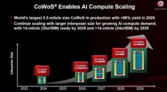
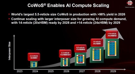
Information disclosed at the Taiwan Semiconductor Manufacturing Company's China Technology Forum indicates that CoWoS (Chip on Wafer on Substrate) serves as the cornerstone for AI training and inference, and its evolution direction is "bigger". Currently, CoWoS with a 5.5 times mask size has achieved mass production, with a yield rate of up to 98%. In the next five years, the CoWoS technology will undergo annual iterations and expand in size to integrate more logic and HBM chips.
It is expected that a 14 times mask size version will be mass-produced in 2028, capable of integrating 20 HBM (High Bandwidth Memory); in 2029, it will further expand to integrate 24 HBM chips. This "giant-scale" packaging capability is aimed at addressing the insatiable demand for memory bandwidth by large-scale AI models.
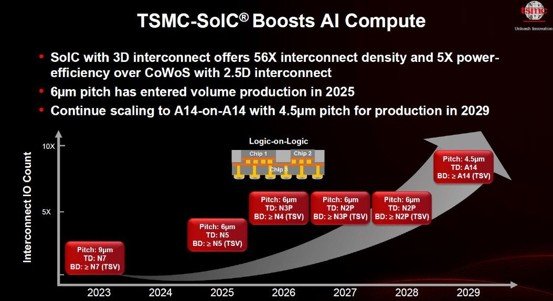
Meanwhile, SoIC (Integrated Chip) represents the "denser" direction. Compared to the 2.5D interconnection of CoWoS, the 3D interconnection technology of SoIC offers 56 times higher interconnection density and 5 times higher power efficiency. As the bonding spacing is reduced from 9 μm to 6 μm and is planned to reach 4.5 μm for A14 stacking in 2029, the vertical transistor connections are becoming as dense as horizontal wiring.
The confidence of the demand side and the concerns of the cost side
What drives this expansion is the visibility of orders driven by AI.
It is reported that as major customers such as Apple, NVIDIA, AMD, Qualcomm and MediaTek increase their order volumes by 10% to 20%, TSMC is accelerating the expansion of its 2nm production capacity. By the end of the year, its monthly production capacity may reach 120,000 wafers, higher than the previous market estimate of 90,000 to 100,000 wafers. The statement made by Senior Vice President Hou Yongqing of TSMC at the North American Technology Forum shows that this year, there are five 2nm factories ramping up production simultaneously, which is the first time in the history of TSMC.
From the perspective of process technology nodes, TSMC predicts that from 2026 to 2028, the production capacity of N2/A16 is expected to rapidly climb at a 70% annual compound growth rate; from 2022 to 2027, the production capacity of N3 and N5 processes will expand at a 25% annual compound growth rate to support the business growth of customers. Thanks to the close team collaboration between the R&D and manufacturing departments, TSMC expects that the wafer production volume of N2 in the first year will be 45% higher than that of N3 at the same period.
At the same time, from 2022 to 2026, the demand for AI accelerators (AI accelerator) from TSMC's customers has increased by 11 times, and the demand for large die wafers has increased by 6 times.
However, the problems at the cost side are also real. The cost of building factories in the United States is approximately 2 to 5 times that of Taiwan, the depreciation cost of wafers is 4 times that of Taiwan factories, and the labor cost is more than twice that of Taiwan factories. Recruiting and cultural adaptation are also long-term issues. Currently, about 2,200 employees come from Taiwan region, and there is also tension between the DEI recruitment requirements and the structure of the engineering team.
Conclusion
Overall, TSMC currently presents a dual-track pattern of "expansion of production capacity in the US and preservation of R&D and advanced packaging in Taiwan". However, what is truly worth continuous tracking may not be the figure of "building several factories", but rather two more fundamental issues: whether the R&D focus on advanced processes can truly remain in Taiwan, and when the economic curve of the US base will converge.